This is my first attempt to build a Bootstrap Loader board for the OMNIBUS.
The mode of operation is largely modelled on the MI8-E (M847). I have some more information about a real MI8-E here.
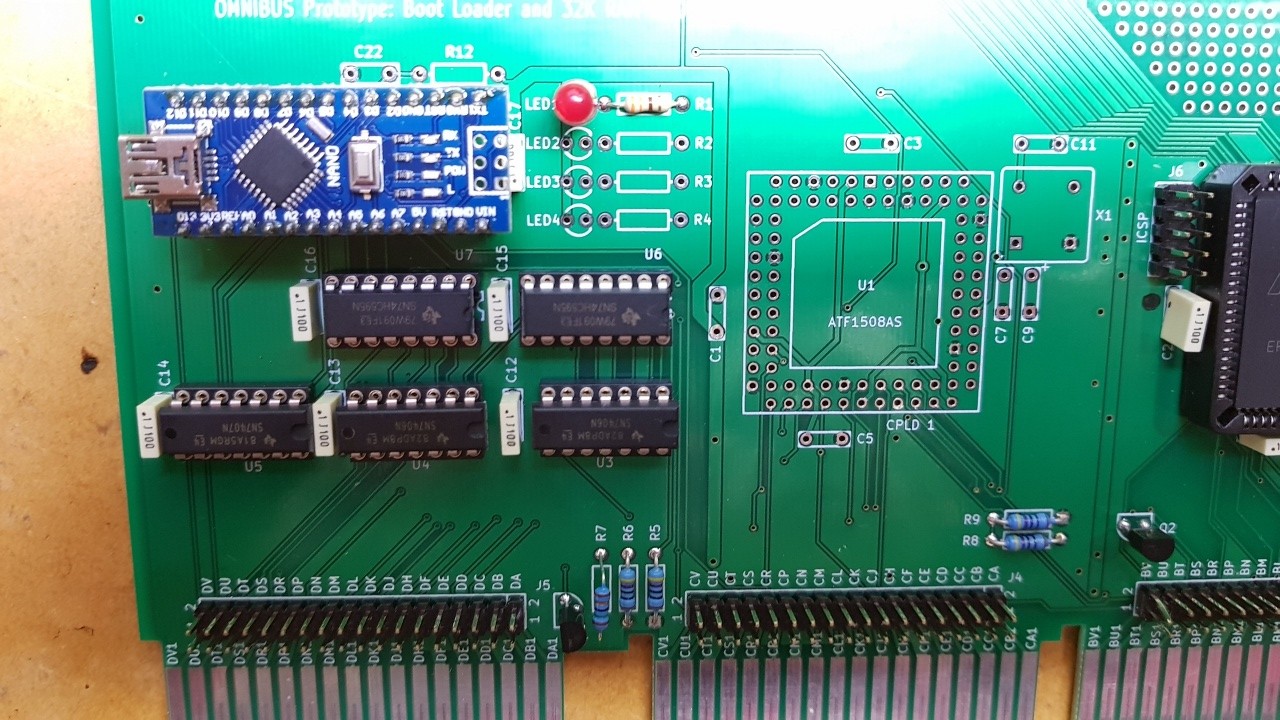
The OMNIBUS Bootstrap Loader Prototype v1.0 has been constructed and is working well (July 2018). It is built on the left-hand side of a dual-purpose prototype board labelled “OMNIBUS Prototype: Boot Loader and 32K RAM V1.0 – www.avitech.com.au”.
It enables the front-panel switch marked “SW” to automatically transfer a device-specific bootstrap loader into the PDP-8’s core memory. The bootstrap loader to be used can be selected using a 4-way dipswitch on the PCB.
Using the v1.0 prototype
The bootstrap loading process is as follows:
- Turn on the PDP-8/e
- Configure the dipswitch settings on the PCB to select the appropriate bootloader
- Confirm the RUN light is off (if it is ON, lower the RUN/HALT switch to the HALT position)
- Raise the RUN/HALT switch to the RUN position
- Lower the SW switch momentarily, and raise it again
By following the above procedure, the selected bootstrap loader will be loaded and will automatically execute.
The dipswitch settings are as follows (using only SW1-5 through SW1-8, down position = 1):
0000 : Reserved
0001 : SerialDisk
0010 : RX01 Units 0 and 1 (long bootloader)
0011 : RX02
0100 : RIM Loader for Low Speed Reader
0101 : MI8-E RIM Loader (Low Speed and High Speed)
0110 : MI8-E TC08
0111 : MI8-E RK8
1000 : MI8-E TD8E
1001 : RL01
1010 : TA8E CAPS-8
1011 : RX01 Unit 0 only (short bootloader)
1100 : RK05 Emulator (2 byte version)
PB1 (nearest to the dipswitch blocks) will boot SerialDisk. PB2 will boot RX01 Unit 0 or Unit 1.
At this stage (3 August 2018) only the SerialDisk and RX01 bootstrap loaders have been successfully tested.
Construction notes
The bootloader portion of the prototype PCB works fine without the 32K RAM section.
The components that you need to fit are shown on the 3rd page of the 4-page PDF.
Some construction notes:
- Omit CPLD1. This was placed on the board as a possible substitute for the 2x74HC595s, 1×7407 and 2x7406s. However I have decided to just go with the 5 TTL ICs instead.
- Omit LED2, LED3, LED4 and associated resistors.
- Omit SW2 (this is used by the 32K RAM section).
- You need only fit a 4-way dipswitch in SW1. Only switches 5, 6, 7 and 8 are connected. Switch 8 is nearest to the unpopulated J7 (40-pin header).
- I recommend removing (from the underside of the Arduino Nano) the diode that feeds in the +5V from the USB port (Vusb). Otherwise the problem is this: If you connect the completed board to your laptop via the USB cable with the board inserted in the Omnibus backplane AND power switched off on the PDP-8, then the USB port will attempt to power the entire Omnibus backplane. It caused smoke to emit from my Nano. Removing the diode fixed this. Perhaps an alternative solution is to place a diode in series with the +5V feed from the PCB to the Arduino Nano (Pin 27 of 30).
- The Arduino software includes support for two optional pushbutton switches. These connect to Arduino “analog” inputs A6 and A7. These PB switches (which I mounted in the prototyping area, with pullup resistors) always launch a bootstrap loader that is “hard coded” into the Arduino source code (ie they are not dipswitch configurable). This allows “SW” to be used for one bootstrap loader (selected by dipswitch), as well as two other dedicated bootstrap loaders via the PB switches. The software currently assigns one of these to SerialDisk, and the other to RX01.
Resources
Here are the design files for this project:
PCB silkscreen layer
PCB composite image
Arduino code (version 17-SEP-2025)
Proposed changes for V2.0
Here is the list of proposed changes for the V2.0 prototype PCB:
- KEY_CONTROL_L, MS_IR_DISABLE_L, LA_ENABLE_L to be driven from 74HC595 and then via 7406 (not 7407)
- /SRCLR inputs to 74HC595s to connect to RESET button of Arduino
- SD-CARD to connect to SPI (and SS) pins of Arduino. Also need to add voltage-divider resistors, and possibly a 3.3V regulator
- Add two dedicated pushbutton switches. Each will always load a particular bootstrap loader. Make provision for external pullup resistors, in case the switches are wired to an off-board location
- Consider reversing the dipswitches, so the right-most (highest numbered) dipswitch connects to the least-significant-bit of the input PORT
- Dipswitch to be 8-way. One side of each switch connects to QA..QH of 74HC595 via a diode (cathode points to 74HC595). Other side of dipswitch bank all connected together and go to an input pin of the Arduino, using internal pullup resistor
- Arduino Nano module will be replaced with an ATmega328P DIL IC
- Add 2 x programming headers (SPI and TTL RS232)
- Fix the bottom-layer silk-screen alignment issue
- Consider adding an output pin that allows SLU1 TXD to be diverted to the Arduino. This will also involve wiring SLU1 TXD to Arduino RXD